 |
       |
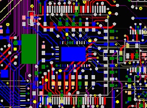
PowerPCB, Pads Layout.
Notes, tips & workarounds:
Combining copper in Layout V2007.
Currently there isn't a way of combining copper features in layout. This
would be useful for example if you want special features on routed copper
layers & especially if you need to mirror them as a block. At the
moment you have to mirror each individual shape & then re-align them
back into the overall shape you want.
This is the workaround. Select each shape in turn & change them to 2D line objects. Then select all of them, right click & 'Combined'. Do the move, rotate or mirror that you need to do, then explode the whole shape, then go back in turn & revert each shape back to copper. Of cause, you'll need to make sure that none of the copper shapes have any nets assigned to them before converting them to a 2D line object.
Test points not showing up in the Paste CAM output:
Occasionally some clients require an unusual paste output with the test
points being shown. In my case we had used TPs as Vias but they would
not show in the paste output. It final stuck me that they will not show
because Vias are PTH. The workaround is to temporarily change the pad
stack of the TP via to NPTH, run the CAM paste output with Test Points
ticked & then set the TP Vias back to PTH.
Text is not appearing in the CAM gerber output preview window?
I’ve had this a few times, we have text on the PCB layers, the layer
is selected in the CAM output, the Text box is ticked as well, to show
text on the plot, but no text is showing in the output preview window.
Chances are then that the text itself is set to Zero width, just go back
in to layout & give the text a width.
Hole in the PCB has a height in IDF?
When importing an IDF from Pads to an mechanical program, quite often
a mounting hole will exhibit a height, when of cause it should be flat,
unless of cause you have a pillar or screw part in its position.
In the Hole part, it simply needs an attribute called HOLE with nothing
typed in the Value. This tells the IDF that it is indeed a hole & requires
no height.
Problem with the license file or running multiple Mentor Software packages:
Run Configurator.exe
For Pads PCB licence location, Pads 2005, in Windows XP it can be found at: C:\Documents and Settings\All Users\Application Data\mgc
Backwards compatible libraries:
Enter library parts into a schematic &/or PCB job, export jobs out as previous ASCII version. Open previous version software & import ASCII files in, select each part in turn, then right click on them & Save to Library.
Via in pad:
Set up your micro via first. Type VP, this should set your default via
to partial. Set filter to Pins only. Select the pins on the device, right
click & add Via at SMD.
 |
|---|
Contact us for availability.
For On or Off site assistance with your PCB
layout design call +44(0)7715 507855
Associated sites:
DCB Automation - Automatic
Optical Inspection for PCB assemblies.
Vivace Lighting - Luminus Products Ltd. LED lighting for architectural, constructional applications, hospitality, commercial and outdoor market places.
| Home | Contact | Profile | Resources | Cadstar | Pads Layout | Pads Logic | Pulsonix | Vutrax | © PCBDEN 2010 |